Introduction
Printed circuit boards have become the essential component of any electronic devices that may include cell phones, car devices, computers and any devices that you use in your daily life. Now they are also being used in digital devices such as clocks and calculators. PCBs are used to control electrical signals within the devices to meet the needs of the mechanical and electrical circuit boards. Within the PCB, there are copper routes that help them manage the flow of electric current across the surface.
This article will discuss crucial steps in the PCB manufacturing process. There are different steps involved in PCB board manufacturing, and each step requires particular attention to detail. The PCB manufacturing starts with the design and then after the design is finalized it goes through the the production of PCB board. Most of the steps in PCB board manufacturing are computerized and machine-driven to avoid human errors and it also rules out the possibility of any incomplete circuits or short circuits. The boards are frequently subjected to various tests so that the quality of the board is not compromised in various stages of the fabrication process. When the final product is made, it is again test before the packaging and transportation.
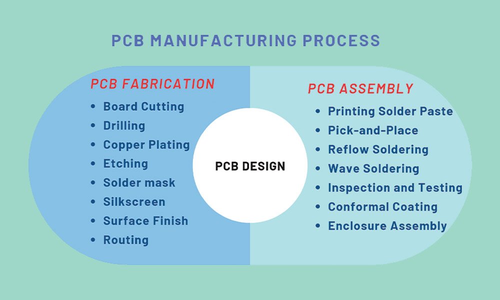
For the simplification we say that there are three main stages in the PCB manufacturing process. The first stage is the design of the board. The next stage refers to the fabrication of the board. And the last stage in PCB manufacturing is PCB assembly. Each stage has different crucial points in PCB manufacturing. This article will cover these points in PCB board manufacturing.
PCB Design Process
The foremost step in the PCB manufacturing process is design prior to the PCB board manufacturing. It includes different steps like
- designing the PCB,
- schematic capture,
- simulation and verification,
- PCB layout and optimization,
- Design rule checking and 3D modelling.
Starting with the initial step in the PCB manufacturing. It requires a plan to start the PCB manufacturing and design. The most common software used in this process is Altium Designer, which is recommended by most experienced engineers and PCB designers. This software contains all the important information needed by the designer such as the number of layers, component notation and number of solder masks. This software encodes the blueprint design for the PCB manufacturing process and it is checked multiple times to make sure there are no errors. After the examination, the design is sent to the next step which is the fabrication process.
PCB Fabrication Process
After the completion of the design, the design is again double checked in the fabrication house with the help of fabricator known as Design for Manufacturability (DFM). After that it is sent to the next stage which is called review of the design. There are different stages involved in the fabrication process for the PCB manufacturing such as:
- Board Cutting
- Drilling
- Copper Plating
- Etching
- Solder mask
- Silkscreen
- Surface Finish
- Routing
- Testing
In the next level, the design is ready to get printed after all the checking has been done by the designer. He makes sure that there would not be any missing parts or structures left unchecked. They don’t print out the design on a regular sheet. Instead, they use a special printer called plotter printer for this process which makes a ‘film’ that is considered as photo negative part. In the PCB board manufacturing two types of inks are used. The black one represents the copper and the non-conductive parts of the PCB are usually represented by the clear one. After the printing of the film, the punch machine makes the hole known as registration hole which is used to align the film in the PCB manufacturing.
After that, the design is printed on the laminating material which is also called the copper foil and then it is printed in the interior layers, which is covered by the photosensitive film called resist. The areas of copper are highlighted with the help of UV radiation to harden the photoresist when copper and resist are lined up. When technician finds no errors in this procedure, the board is passed on the next level in PCB board manufacturing. Then next in fabrication process chemical etching is used to remove extra copper.
Multi-layer boards are composed of multiple layers of copper traces, normally more than three layers. And each copper layers are separated by dielectric. It adds more layers of copper and dielectric to stackups. The PCB manufacturing process has extra steps during the stage of the fabrication to cover other layers of the board. For each layer of the board every step is repeated again.
The type of dielectric material used between those copper layers has a direct effect on signal integrity, especially in high-frequency applications. Engineers working on RF or high-speed digital boards often turn to dielectric-constant plastics with low permittivity values to reduce signal loss and crosstalk between traces. Selecting the right dielectric early in the stackup design stage prevents performance issues that are difficult and costly to correct once fabrication is underway.
The cleansing of each layer of the board takes place and after that they are sent to the optical inspection and layer alignment. The AOI in the PCB manufacturing makes sure that each layer meets the design requirement. After that there is the application of solder mask but the panels are required to be cleaned properly for its application.
Next on the step of PCB manufacturing process is the silkscreen application and surface finish application. It is referred to as the important data that is fabricated on the board in the fabrication process. It may include part numbers and components notations mainly.
The PCB boards are then subjected to testing after all the essential measures have been taken. The test is called the electrical reliability test. It must follow the standards of IPC-9252. If it has passed the electrical test and any other test chosen by the engineers, then it passed on the next stage which is routing out and inspection. Thermal shock of 288 degrees requires for 10 seconds for high frequency PCB fabrication.

PCB Assembly Process
The next in the PCB manufacturing process is the board assembly. It also follows different steps such as
- Printing Solder Paste
- Pick-and-Place
- Reflow Soldering
- Wave Soldering
- Inspection and Testing
- Conformal Coating
- Enclosure Assembly
The assembly of the PCB can be done through two processes, SMT & THT. The SMT process has different steps which includes solder paste printing, inspection, placing components, X-ray inspection, reflow soldering and AOI. If there are holes after the SMT assembly then it has to follow the PTH assembly which has different steps including wave soldering, trimming leads and visual checks.
In the first step the solder paste gets printed into pads and then with the help of pick and place machine the components are placed on the pads. Then they are passed through the reflow soldering oven to melt the paste in the PCB manufacturing process which helps to secure the components. The final step is to integrate the PCB into plastic or metal product with the help of pins, clips and fasteners. Now before packaging and shipping they must undergo the final inspection which is done with the help of AOI and other techniques.
Effective PCB Manufacturing Process
If you want to implement effective PCB manufacturing process, you have to make sure of the following important points.
File Formats Compatible
Both groups OEM & CM should have the same file formats to have the connection between them in the PCB board manufacturing.
Design for Manufacturing
It will make sure that the design would pass through all the stages of fabrication in the PCB manufacturing. It is the important factor in the entire process.
Select Suitable PCB Materials
You should have to negotiate with the manufacturer on the materials of the PCB board to make it cost-effective and less time-consuming. Both parties must agree on the same board material.
On Time Components Sourcing
You have to make sure that the fabricator has all essential components needed for the PCB manufacturing and assembly process so that the procedure could go on smoothly.
Strictly Quality Control
Enough experienced quality staff are needed to check in PCB manufacturing process to make sure all PCBs meet the industrial standards and customers’ requirement.
Conclusion
We have discussed all the important factors in PCB manufacturing process from initial designs to the assembly of the components. The manufacturing of PCB could be very difficult and complex procedure and each step should be executed carefully. The process may be extended to further 20 or more steps depending on the layers of board and complexity involved in the process. Strict adherence to the necessary protocols would result in high-quality boards that satisfy functionality requirements.
Also read: Harnessing the Power of PCB-PCBA Collaboration in Electronics


