Mirror Review
June 26, 2026
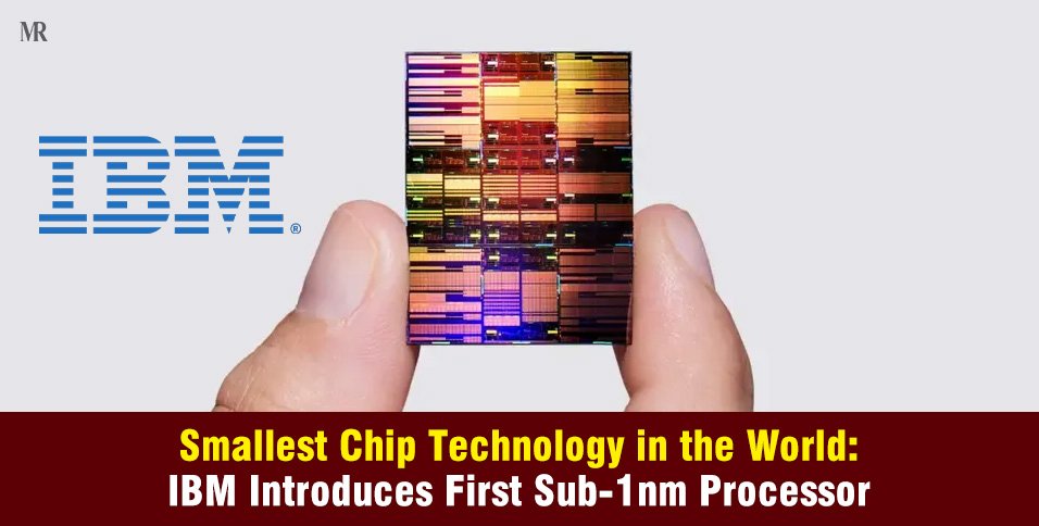
IBM has unveiled the world’s first sub-1-nanometer chip technology, marking a massive milestone in semiconductor physics. This new process packs nearly 100 billion transistors onto a piece of silicon the size of a fingernail by using a 0.7-nanometer (7 angstrom) node design. IBM’s smallest chip technology in the world addresses the growing need for high-efficiency hardware to power demanding AI workloads and global computing infrastructure. Moving past traditional physical scaling limits, this development establishes a clear path for hardware engineering over the next decade.
Inside IBM’s Sub-1nm Chip
The semiconductor industry has spent decades shrinking transistors to pack more computing power into tight spaces. As sizes approach the atomic level, traditional manufacturing methods run into severe physical constraints. IBM solved this bottleneck by transitioning from two-dimensional layouts to a vertical architecture.
The first sub-1-nanometer node chip relies on three major innovations:
- Ultra-thin dielectric wafer bonding: A highly precise manufacturing technique that joins two separate wafers into a unified, multilayered structure with minimal physical defects.
- Dual-channel engineering: An optimized gate-stack design where the NFET and PFET channels operate independently, allowing engineers to maximize performance for each layer.
- SRAM scaling: A design update that shrinks static random-access memory footprints by 40%, cramming far more memory capacity into the same physical space.
By moving to the 0.7 nm generation, IBM’s sub-1 nm chip doubles the transistor density compared to its own 2-nanometer technology introduced in 2021.
For comparison, a human red blood cell spans roughly 7,000 nanometers, making it 10,000 times wider than one of these new 7 angstrom transistor nodes.
Driving AI with Nanostack 3D Chip Architecture
The foundation of the smallest chip technology in the world is the nanostack 3D chip architecture.
In 2015, IBM pioneered nanosheet technology, which became the standard for 3 nm and 2 nm processors. The new nanostack design takes that concept further by stacking and staggering nanosheet transistors vertically along the z-axis.
This vertical stacking allows chip designers to use entirely different material combinations on different layers. As a result, each transistor can be tuned independently for peak efficiency.
This structural shift provides a significant boost in processing capability while drastically lowering electricity consumption.
Comparing Generations: 2nm vs. World’s First Sub-1 Nanometer Chip Technology
The shift to the smallest chip technology in the world brings massive advantages over previous top-tier components. The following data highlights the performance jump from the older 2 nm platform to the new 0.7 nm nanostack architecture:
| Performance Metric | IBM 2 nm Chip (2021) | IBM Sub-1 nm Chip (2026) |
| Transistor Count (Fingernail Size) | ~50 Billion | ~100 Billion |
| Node Measurement | 2 nanometers | 0.7 nanometers (7 Angstroms) |
| Performance Gain | Baseline | Up to 50% Higher |
| Energy Efficiency | Baseline | Up to 70% Reduction in Power |
| SRAM Area Reduction | Baseline | 40% More Space-Efficient |
This 40% memory reduction directly targets data bottlenecks in AI hardware. Fast, on-chip SRAM cache is critical for modern AI accelerators. By squeezing more memory next to the logic gates, data moves much faster, preventing the processor from sitting idle while waiting for information.
Real-World Impact on Computing and AI
The massive efficiency gains of IBM’s sub-1 nm chip change what is possible for large-scale computing. Today’s premier AI accelerators output around 1,500 trillion operations per second (TOPS). IBM estimates that a system built with this 1 nm process could achieve nearly 9,000 TOPS, a sixfold increase in processing speed.
This processing power could rewrite timelines for complex technical tasks:
- Faster LLM Training: Training a massive, frontier AI model currently takes about three months. Using 7 angstrom hardware could cut that timeline down to just a couple of weeks.
- Lower Data Center Power Costs: Data centers consume vast amounts of electricity. A 70% reduction in power use helps tech companies scale up cloud infrastructure without overwhelming local power grids.
- Longer Battery Life: For edge devices, robots, and remote sensors, these efficiency gains mean devices can run complex programs locally while requiring far fewer recharges.
“IBM’s latest chip breakthrough marks a landmark moment in computing, pushing technology beyond the nanometer era to the scale of atoms. With our new nanostack architecture, we’re not just making smaller transistors, we’re reinventing how chips are built to deliver dramatically more power and energy efficiency,” said Jay Gambetta, Director of IBM Research and IBM Fellow.
The Road to Commercial Production
While the laboratory results are fully verified, bringing the smallest chip technology in the world to commercial markets will take some time. IBM functions as a research and design leader rather than operating its own mass-production factories. The company envisions a clear path to commercial production within the next five years.
Historically, major chip manufacturers like TSMC, Samsung, and Intel have licensed and productized IBM’s node designs. IBM has also collaborated closely with ecosystem partners like Lam Research, Tokyo Electron, and SCREEN Semiconductor Solutions. These teams are currently working at an Albany, New York research facility to master High Numerical Aperture Extreme Ultraviolet (High NA EUV) lithography. This ultra-precise printing tech from ASML is absolutely necessary for etching circuits at an atomic scale.
Furthermore, IBM plans to create Anderon, which will operate as the world’s first pure-play quantum foundry. This move ensures that advanced wafer manufacturing capabilities remain a central focus as the industry transitions into the angstrom era.
End Note
IBM’s successful demonstration of the smallest chip technology in the world is a big win for the semiconductor industry. By stacking components vertically with nanostack 3D chip architecture, engineers have bypassed the physical limits that threatened to stall Moore’s Law.
While consumers will wait a few years to see these 0.7 nm processors inside commercial devices, this milestone ensures that the next decade of AI, cloud infrastructure, and consumer electronics will continue to grow faster and more energy-efficiently.
Maria Isabel Rodrigues